- 您现在的位置:买卖IC网 > Sheet目录317 > C8051F380-TB (Silicon Laboratories Inc)DEV KIT FOR C8051F38X
�� �
�
�C8051F380/1/2/3/4/5/6/7/C�
�22.5.3.� Write� Sequence� (Slave)�
�During� a� write� sequence,� an� SMBus� master� writes� data� to� a� slave� device.� The� slave� in� this� transfer� will� be�
�a� receiver� during� the� address� byte,� and� a� receiver� during� all� data� bytes.� When� slave� events� are� enabled�
�(INH� =� 0),� the� interface� enters� Slave� Receiver� Mode� when� a� START� followed� by� a� slave� address� and� direc-�
�tion� bit� (WRITE� in� this� case)� is� received.� If� hardware� ACK� generation� is� disabled,� upon� entering� Slave�
�Receiver� Mode,� an� interrupt� is� generated� and� the� ACKRQ� bit� is� set.� The� software� must� respond� to� the�
�received� slave� address� with� an� ACK,� or� ignore� the� received� slave� address� with� a� NACK.� If� hardware� ACK�
�generation� is� enabled,� the� hardware� will� apply� the� ACK� for� a� slave� address� which� matches� the� criteria� set�
�up� by� SMB0ADR� and� SMB0ADM.� The� interrupt� will� occur� after� the� ACK� cycle.�
�If� the� received� slave� address� is� ignored� (by� software� or� hardware),� slave� interrupts� will� be� inhibited� until� the�
�next� START� is� detected.� If� the� received� slave� address� is� acknowledged,� zero� or� more� data� bytes� are�
�received.�
�If� hardware� ACK� generation� is� disabled,� the� ACKRQ� is� set� to� 1� and� an� interrupt� is� generated� after� each�
�received� byte.� Software� must� write� the� ACK� bit� at� that� time� to� ACK� or� NACK� the� received� byte.�
�With� hardware� ACK� generation� enabled,� the� SMBus� hardware� will� automatically� generate� the� ACK/NACK,�
�and� then� post� the� interrupt.� It� is� important� to� note� that� the� appropriate� ACK� or� NACK� value� should� be�
�set� up� by� the� software� prior� to� receiving� the� byte� when� hardware� ACK� generation� is� enabled.�
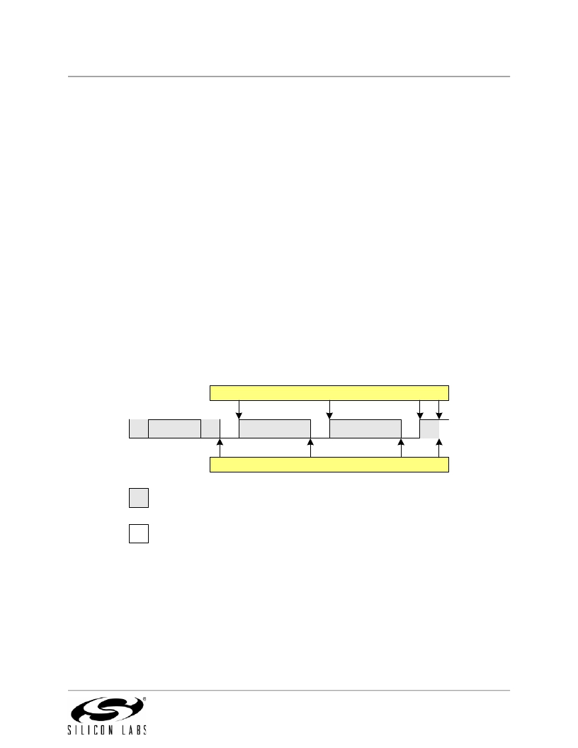
�The� interface� exits� Slave� Receiver� Mode� after� receiving� a� STOP.� The� interface� will� switch� to� Slave� Trans-�
�mitter� Mode� if� SMB0DAT� is� written� while� an� active� Slave� Receiver.� Figure� 22.7� shows� a� typical� slave� write�
�sequence.� Two� received� data� bytes� are� shown,� though� any� number� of� bytes� may� be� received.� Notice� that�
�the� ‘data� byte� transferred’� interrupts� occur� at� different� places� in� the� sequence,� depending� on� whether� hard-�
�ware� ACK� generation� is� enabled.� The� interrupt� occurs� before� the� ACK� with� hardware� ACK� generation� dis-�
�abled,� and� after� the� ACK� when� hardware� ACK� generation� is� enabled.�
�Interrupts� with� Hardware� ACK� Enabled� (EHACK� =� 1)�
�S�
�SLA�
�W�
�A�
�Data� Byte�
�A�
�Data� Byte�
�A�
�P�
�Interrupts� with� Hardware� ACK� Disabled� (EHACK� =� 0)�
�Received� by� SMBus�
�Interface�
�Transmitted� by�
�SMBus� Interface�
�S� =� START�
�P� =� STOP�
�A� =� ACK�
�W� =� WRITE�
�SLA� =� Slave� Address�
�Figure� 22.7.� Typical� Slave� Write� Sequence�
�Rev.� 1.4�
�225�
�发布紧急采购,3分钟左右您将得到回复。
相关PDF资料
C8051F912DK
KIT DEV FOR C8051F91X/C8051F90X
C8051F930-TB
BOARD TARGET/PROTO W/C8051F930
C8051T610DB24
DAUGHTER BOARD T610 24QFN SOCKET
C8051T630DB20
BOARD SOCKET DAUGHTER 20-QFN
CAN-100
BOARD EVAL RS232 100QFP
CANADAPT28
KIT ADAPTER CANDEMOBOARD 28PLCC
CAT24AA01WI-GT3
IC EEPROM SERIAL 1KB I2C 8SOIC
CAT24AA02WI-G
IC EEPROM SERIAL 2KB I2C 8SOIC
相关代理商/技术参数
C8051F381
制造商:SILABS 制造商全称:SILABS 功能描述:USB DRIVER CUSTOMIZATION
C8051F381-GM
功能描述:8位微控制器 -MCU USB-64K-Flash
RoHS:否 制造商:Silicon Labs 核心:8051 处理器系列:C8051F39x 数据总线宽度:8 bit 最大时钟频率:50 MHz 程序存储器大小:16 KB 数据 RAM 大小:1 KB 片上 ADC:Yes 工作电源电压:1.8 V to 3.6 V 工作温度范围:- 40 C to + 105 C 封装 / 箱体:QFN-20 安装风格:SMD/SMT
C8051F381-GMR
功能描述:8位微控制器 -MCU USB-Flash-64k-ADC RoHS:否 制造商:Silicon Labs 核心:8051 处理器系列:C8051F39x 数据总线宽度:8 bit 最大时钟频率:50 MHz 程序存储器大小:16 KB 数据 RAM 大小:1 KB 片上 ADC:Yes 工作电源电压:1.8 V to 3.6 V 工作温度范围:- 40 C to + 105 C 封装 / 箱体:QFN-20 安装风格:SMD/SMT
C8051F381-GQ
功能描述:8位微控制器 -MCU USB-64K-Flash
RoHS:否 制造商:Silicon Labs 核心:8051 处理器系列:C8051F39x 数据总线宽度:8 bit 最大时钟频率:50 MHz 程序存储器大小:16 KB 数据 RAM 大小:1 KB 片上 ADC:Yes 工作电源电压:1.8 V to 3.6 V 工作温度范围:- 40 C to + 105 C 封装 / 箱体:QFN-20 安装风格:SMD/SMT
C8051F381-GQR
功能描述:8位微控制器 -MCU USB-Flash-64k-ADC RoHS:否 制造商:Silicon Labs 核心:8051 处理器系列:C8051F39x 数据总线宽度:8 bit 最大时钟频率:50 MHz 程序存储器大小:16 KB 数据 RAM 大小:1 KB 片上 ADC:Yes 工作电源电压:1.8 V to 3.6 V 工作温度范围:- 40 C to + 105 C 封装 / 箱体:QFN-20 安装风格:SMD/SMT
C8051F382
制造商:SILABS 制造商全称:SILABS 功能描述:USB DRIVER CUSTOMIZATION
C8051F382-GQ
功能描述:8位微控制器 -MCU USB-Flash-32k-ADC
RoHS:否 制造商:Silicon Labs 核心:8051 处理器系列:C8051F39x 数据总线宽度:8 bit 最大时钟频率:50 MHz 程序存储器大小:16 KB 数据 RAM 大小:1 KB 片上 ADC:Yes 工作电源电压:1.8 V to 3.6 V 工作温度范围:- 40 C to + 105 C 封装 / 箱体:QFN-20 安装风格:SMD/SMT
C8051F382-GQR
功能描述:8位微控制器 -MCU USB-Flash-32k-ADC RoHS:否 制造商:Silicon Labs 核心:8051 处理器系列:C8051F39x 数据总线宽度:8 bit 最大时钟频率:50 MHz 程序存储器大小:16 KB 数据 RAM 大小:1 KB 片上 ADC:Yes 工作电源电压:1.8 V to 3.6 V 工作温度范围:- 40 C to + 105 C 封装 / 箱体:QFN-20 安装风格:SMD/SMT